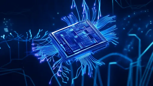
The realm of wireless communication is on the cusp of a transformative leap as researchers and engineers turn their attention to terahertz (THz) frequencies. These ultra-high frequencies, ranging from 0.1 to 10 THz, promise unprecedented data rates and bandwidth, potentially revolutionizing applications from 6G networks to advanced imaging systems. However, the design of THz communication chips presents a formidable array of challenges that must be overcome to unlock this potential.
The Physics of Terahertz: A Double-Edged Sword
At the heart of THz chip design lies a fundamental tension between opportunity and limitation. The same properties that make terahertz frequencies attractive—their ability to carry vast amounts of data—also make them exceptionally difficult to harness. Unlike their microwave counterparts, THz signals suffer from severe atmospheric attenuation, particularly due to water vapor absorption. This creates what researchers colloquially refer to as "terahertz gaps" where signal propagation becomes problematic. Chip designers must therefore create systems that can not only generate and detect these faint signals but also compensate for their rapid degradation in real-world environments.
Material Limitations at Microscopic Scales
Conventional semiconductor materials used in lower-frequency chips begin to show their limitations when pushed into the terahertz regime. Silicon, the workhorse of modern electronics, suffers from increased loss and reduced efficiency at THz frequencies. This has spurred investigations into alternative materials like indium phosphide (InP) and gallium nitride (GaN), which offer better high-frequency performance but come with their own manufacturing challenges. The search for optimal materials extends to packaging as well, where traditional insulators can become lossy at THz frequencies, requiring novel dielectric solutions.
The Miniaturization Paradox
As with all electronics, there's constant pressure to make THz components smaller, but the laws of physics present unique hurdles at these frequencies. The wavelength of THz radiation ranges from 3 mm to 30 μm—orders of magnitude smaller than microwave frequencies. This means that traditional circuit elements like transmission lines and antennas must be correspondingly miniaturized, pushing the limits of current fabrication technologies. Moreover, at these scales, quantum effects and parasitic phenomena that were negligible at lower frequencies become dominant considerations in chip design.
Power Generation and Efficiency Challenges
Generating sufficient power at terahertz frequencies remains one of the most significant obstacles. Traditional electronic approaches struggle to produce usable power levels, while optical methods like photomixing often require complex external laser systems. This power challenge extends throughout the signal chain—from oscillators and amplifiers to modulators and detectors. Each component must be optimized not just for performance but for power efficiency, particularly for portable or battery-powered applications where thermal management becomes critical at these high frequencies.
Integration: Bringing It All Together
Perhaps the most daunting challenge lies in system integration. A functional THz communication chip must combine high-frequency analog components with sophisticated digital signal processing—all while managing heat dissipation, cross-talk, and power distribution. This requires co-design approaches that break down traditional boundaries between RF, analog, and digital design domains. Emerging techniques like heterogeneous integration, where different technologies are combined at the package level, show promise but add complexity to an already challenging design process.
The Road Ahead: Innovation Through Constraint
Despite these challenges, progress in THz chip design continues at a remarkable pace. Researchers are exploring innovative architectures like plasmonic circuits that exploit surface waves, while advances in nanofabrication enable previously impossible structures. Machine learning is being applied to optimize component design and compensate for signal impairments. As these technologies mature, they promise to overcome the current limitations, potentially ushering in a new era of ultra-high-speed wireless communication that could transform everything from medical diagnostics to satellite networking.
The journey toward practical terahertz communication chips exemplifies the iterative nature of technological progress—where each solved problem reveals new challenges, and each challenge overcome opens doors to previously unimaginable applications. While significant hurdles remain, the collective efforts of materials scientists, device physicists, and circuit designers worldwide continue to push the boundaries of what's possible at these fascinating frequencies.

By /Jul 11, 2025

By /Jul 11, 2025

By /Jul 11, 2025

By /Jul 11, 2025
By /Jul 11, 2025

By /Jul 11, 2025

By /Jul 11, 2025

By /Jul 11, 2025

By /Jul 11, 2025

By /Jul 11, 2025

By /Jul 11, 2025

By /Jul 11, 2025

By /Jul 11, 2025

By /Jul 11, 2025

By /Jul 11, 2025
By /Jul 11, 2025

By /Jul 11, 2025
By /Jul 11, 2025